NANOENGINEERING OF ELEMENTAL BASE OF PHOTONICS
|
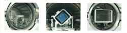
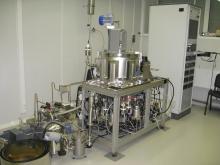
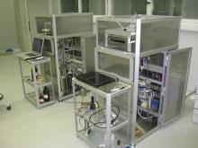
I. Elemental base of photonic superprocessor Fundamental properties of galvanic communication channels of electronic computers restrict productivity of electronic computers on the level far from the level needed for supercomputer information technologies aimed at solution of state-scale problems of social-economic and military predictions. A limited bandwidth, impossibility of spatial crossings, arising cross-talks at ultradense arrangement of logical elements, known under total name of “problem of links”, do not allow one to make use, in full measure, of either achievements of technology in improvement of speed of logical elements, or possibilities to increase productivity of electronic computers by passing from the conventional Neimann-type architecture to parallel architectures with dynamic links. As the main and, at present, the only real way to solve the problem of links, is considered replacement of electric communication channels by optical ones, with the role of information carrier played by spatiotemporal packets of light quanta (photons). Ability of photons to travel in free space with no cross-talks and to transfer information in a great number of parallel broadband (~1015 Hz) of information channels, the feasibility of total connectivity with virtually unlimited number of elements by the methods of diffraction optics and holography, leave optics beyond any competition upon designing of parallel computational systems with dynamic links. Fundamental scientific and technological problem whose solution is capable of transeffing multibillion investments from supercomputer electronics to photonics consists in creation of photonic logic gates and memory cells which can substantially exceed, in terms of the system factor, the properties of similar electronic elements. The main problem is that to achieve the required paramenets, it is necessary to creat nonlinear optical media that combine properties unachievable for materials obtained in the frame of traditional macrotechnologies. Theoretical, experimental and technological studied performed by the participants of the project during the last decase led them to the conclusion that the up-to-date technology of nanoengineering makes it possible to approach to practical solution of the problem of creation of the photonic logic elements substantially exceeding their electronic analogs and admitting their use both in classical (bit-type) and in quantum (qubit-type) computational systems. The task of the project is to demonstrate this possibility and to determine real ways for optimization of operational parameters of these elements. Physico-technological approaches to the project are based on two possibilities to create the photonic gate arrays and the arrays of photonic memory on the basis of epitaxial heterostructures. - The first of them consists in in nanoengineering of quantu, mirrors with the properties of two-dimensional (2D) reqular ensembles of two-level (TL) systems of optical range – 2D-TL-structures of photonic logic. - The second possibility is related to nanoengineering of quantum mirrors with the properties of quasi-2D reqular ensembles of three-level -systems of optical range with pure spin ground state - 2D- structures of photonic memory. Based on the results of studies of recent years, the authors of the project hace managed to formuilate the requirements to spectroscopic and kinetic parameters of the medium suitable for creation of photonic switch. To obtain the greatest speed in the two-level and thre-level systems, the optimal are considered to be laterally confines excitons and trions of quasi-2D semiconductor heterostructures, respectively. Estimates based on the results of the experimental studies [4-6] have shown that, under condition of minimization of the inhomogeneous broadening to the value smaller than the radiative width, the GaAs/AlGaAs-based quasi-2D epitaxial structure can be considered as the best basic structures for creation of the photonic gate arrays [7-8]. The above ideology practically determines the main technological stages of nanoengineering of the functional photonic heterostructures. The most important of these stages are: 1. Grosing by the method of molecular beam epitaxy (MBE) of 2D-excitonic and 2D-trionic quantum mirrors – basic semiconductor heterostructures with isolated quantum wells, characterized by the limiting low fluctuations of the z-quantized potential (Fig. 1). Fig. 1a. Morphology of a quantum mirror with an isolated quantum well. Fig. 1b. Energy structure of a quantum mirror. 2. Nanofragmentation of nominally pure and n-doped quantum mirrors by methods of nanolithography to provide them properties of functional structures of photonic logic and memory with 2D-TL and 2D- spectra of eigenstates, respectively (Fig. 2). Fig. 2. Nanofragmentation: For GaAs: In the proposed configuration, the plane quasi-2D heterostructure will represent an array of elements of photonic logic (memory) operating in parallel. The limiting switching rate will be determined by the time of radiative recombination of the excitons, which, in such structures, makes up units of picosecond [10], whereas the linear size of an elementary gate element has the order of the light wavelemgth, i.e., fractions of μm. It means that in an area of 1 mm2 there may be arranged up to 106 of elements operating in parallel, with each of them being capable of switching with the frequency up to 1011 Hz. The energy consumption to one logical operation can be reduced to 10-17 J, i.e., down to the value incomparably small compared with that for the present-day electronic logical elements. It is important that, in contrast to any electronic scheme, in the developed logic elements, which are, in essence, photonic analogs of the Feynman quantum gate [11], the switching energy does not dissipate in the material of the switch, but is rather converted to the output signal. This fact practically completely cancels one more problem of the super-high-speed p[rocessors – the problem of heat removal. For the present moment, the main goal is to directly prove the feasibility of the photonic gate arrays and photonic memory arrays based of quasi-2D semoconductor heterostructure. Present-day status of the qork. The main results of the work of the team, leading it to the row of the world leaders of this trend are: - Development of technology of epitaxial growth of the 2D-excitonic quantum mirrors with fluctuations of the z-quantizing potential minimized on the level of theoretical limit. This resord result virtually provides the speed of the photonic logic on the claimed level [9]; - Development of the technology of epitaxial growth of the 2D-trionic quantum mirrors and discovery, in these mirrors, of the effect of optical orientation of spins of resident carriers and possibility of the electric-field-control of the spin-polarization relaxation time. These results prove findamental opportunity of creation of the operative photonic memory [9,10]. Practical importance of the above resilts is that they in fact transferred the problem of creation of the photonic logic and memory nanostructires to the final technological level – the level of the technology of the lateral regular nanofragmentation. The above results have been obtained after extensive work on modernization of the domestic MBE-machine EP-1302 and development of adequate methodology and equipment for femtosecond characterization of functional parameters of epitaxial heterostructures. The qork planned to the nearest future are supposed to be carried out along two lines. The goal of the first direction is the development of technology of creation of 2D-excitonic (2D-trionic) quantum mirrors with optical susceptibility of the free 2D-excitonic (2D-trionic) layer – as the basic epitaxial structures for the technology of the lateral nanofragmentation. This problem includes: parfection of the growth regimes of the MBE technology to the level of a high technological reproducibility and development of the technology of deposition to the structure surface of an antireclection layer with no destruction of the Z-quantizing potential of the quantum well. The goal of the second direction is the development of the technology of nanofragmentation, To solve this problem, we will have to solve (along the technological problems proper) the problem of development and creation of the needed equipment of nanolithography (or its purchasing from foreign manufacturers). In spite of the fact that the above developments refer to the sphere of interests of the country and are funded by state budget, we find it unrealistic to obtain the financial support needed for purchasing the above equipment from the budget of Russian Federation. For the present moment, as the only realistic variant, we consider the development and creation of the equipment using our own potentialities. Perhaps, it is not the most reasonable way, but taking into account professional qualification of the team, this way is the most realistic. Anticipated difficulties are mainly related to the fact that both the planned and already obtained technological results can hardly be directly transferred to the level of industrial technologies, because they are achieved by the researchers of the highest qualification with nonstandard equipment. It is clear that the most direct (and, perhaps, the only correct) way to overcome the gap between the experimental and industrial technologies is to carry out the technological developments on the up-to-date equipment adapted to industrial manufacturing. This way requires, however, great one-time financial investments. Main risks are related not to the probability of fundamentally technological non-achievment of the result (this probability is rather small and, according to our estimates, lies in the range of 5-10 %), but rather to the fact that practical application of the developed elements of the supercomputer technology may take a few years and thus to freeze original investments. There is, however, a good way to make oneself safe with respet to these risks. The point is that the technologies to be developed have a wide spectrum of application upon production of commercially attractive items. Among them are so well known, but absent on the domestic market items of military application as array detectors of IR range 8 – 12 μm on heterostructures with quantum wells (QWIP), hogh-power microwave transistors on heterostructures with 2D electron gas (HEMT), as well as a set of useful devices based on the effect of optical conjunction found by us in semiconductor epitaxial structures. II. Epitaxial structures with the function of analog optical conjunction. The effect of analog optical conjumction (analog optical logic summation) consists in the following: upon illumination of a given spot of a heterostructure by two light sources with the spectral composition matching the photoelectric sensitivity of the structure heterolayers, the heterostructure prodices a photoelectric signal that obeys the table of a double-input logic gate “AND”. As was shown in our studies, this effect can be used upon design of a wide class of fundamentally new devices (photovidicons of the visible and IR range, optically addressed memory, etc.) [10]. All these devices are patent-pure and their production, taking into accound possibility of double application, has good economical prospects. References 1. Yu.K.Dolgikh, S.A.Eliseev, Yu.P.Efimov, A.A.Fedorov, I.Ya.Gerlovin, G.G.Kozlov, V.V.Ovsyankin, V.V.Petrov, B.V.Stroganov, V.S.Zapasskii, "Spectroscopic and structural aspects of femtosecond dynamics of reflectivity of AlGaAs/GaAs superlattices", in "Nanostructures: physics and technology", Proc. 6th Int. Simp. June 22-26, 1998, St.Petersburg, Russia, p.370 2. G.G.Kozlov, Yu.K.Dolgikh, Yu.P.Efimov, S.A.Eliseev, A.A.Fedorov, I.Ya.Gerlovin, V.V.Ovsyankin, B.V.Stroganov, and V.S.Zapasskii, "Quantum Beats Between the Fine- Structure States of Localized HH-excitons in GaAs/AlGaAs Superlattices", in "The Physics of Semiconductors", ed. D.Gershoni, World Scientific Publ., Singapoure, 1999, CD-ROM, No. 1462. 3. I.Ya.Gerlovin, V.V.Ovsyankin, B.V.Stroganov, V.S.Zapasskii, "Nonlinear optical dynamics of semiconductor nanostructures - feasibility of the photonic quantum gate", Journ. of Lumin., 87-89, (2000), 421-422 4. I.Ya.Gerlovin, V.V.Ovsyankin, B.V.Stroganov, V.S.Zapasskii, "Coherent transients in semiconductor nanostructures as the base of optical logic operating" in "Nanostructures: Physics and Technology", Proc. 8th Int.Simp. June 19-23, 2000, Ioffe Institute, St.Petersburg, Russia, p.530-533. 5. I.Ya.Gerlovin, V.V.Ovsyankin, B.V.Stroganov, V.S.Zapasskii, "Coherent transients in semiconductor nanostructures as a basis for optical logic operating", Nanotechnology, 11 (2000), 383-386. 6. E. Ubyivovk, Yu. K. Dolgikh, Yu. P. Efimov, S. A. Eliseev, I. Ya. Gerlovin, I. V. Ignatiev, V. V. Petrov, and V. V. Ovsyankin, "Spectroscopy of high-energy excitonic states in ultra-thick GaAs quantum wells with a perfect crystal structure", J. Lumin., 102-103, 751-754 (2003). 7. V. V. Ovsyankin, B.V. Stroganov, Yu. K. Dolgikh, S. A. Eliseev, V. V. Petrov and V. S. Zapasskii, “Quantum switching of modes of spontaneous emission and dynamics of spatial interferenceof 2D excitons” in NANOSTRUCTURES: Physics and Technology, p.24, (2004), Ioffe Institute, St Petersburg. 8. Yu. Verbin, Yu. P. Efimov, I. V. Ignatev, V. V. Petrov, Yu. K. Dolgikh, S. A. Eliseev, I. Ya. Gerlovin, V. V. Ovsyankin, and Y. Masumoto, "Spin memory in the n-doped GaAs/AlGaAs quantum wells.", SPIE, v. 5023, pp. 432-435 (2003). 9. I.Ya.Gerlovin, Yu.K.Dolgikh, S.A.Eliseev, V.V.Ovsyankin, Yu.P.Efimov, I.V.Ignatiev, V.V.Petrov, S.Yu.Verbin, Y.Masumoto, “Spin dynamics of carriers in the GaAs quantum wells in an external electric field.”. Phys. Rev. B 69, 035329 (2004) 10. G.G.Kozlov, Yu.K.Dolgikh, Yu.P.Efimov, S.A.Eliseev, V.V.Ovsyankin, and V.V.Petrov, “Optical vidicon based on a leyered semiconductor structure: Image readout and storage”, Zh. Tekh.Fiz., v. 74, no. 6, p.p. 65-69, 2004. The team of the participants сomprises 22 persons including two Doctors of Sciences, 13 Candidates of Sciences, two post-graduate students, and three students. List of equipment available for the fulfillment of the work. 1. Technological and analytical facility of Molecular Beam Epitaxy EP-1302. 2. Technological and analytical facility of Molecular Beam Epitaxy “Katun”. 3. System of laser equipment for pulsed holography EMG 1003+ FL 3002 (Lambda Physik). 4. Ewuipment for stationary optical spectroscopy: - Raman and PL spectrometer on the basis of the monochromator U1000 (Jobin-Yvon), - Multichannel high-resolution reflection spectrometer on the basis of 2-m spectrograph DAS with tunable source of stationary laser emission (home made Ti-sapphire) and ССD-matrix detector Hamamatsu Photonics. 5. Facility of the femto- and picosecond pulse spectroscopy of delayed optical collisions on the basis of a femto- and picosecond Ti-Sapphire laser Tzunami (Spectra Physics). 6. Facility of nondegenerate laser spectropolarimetry and modeling of the photonic logic and memory elements on the basis of two highly stable tunable semiconductor lasers LYNX –120 (Saher). 7. Equipment for low-temperature studies: helium closed-loop cryostats and cryostats with superconducting magnets.
|

 Загрузить PDF-версию № 11
 Загрузить PDF-версию № 10
 Загрузить PDF-версию № 9